

Products
Green and environmentally friendly new enterprise of polymer composite materials
Semiconductor field
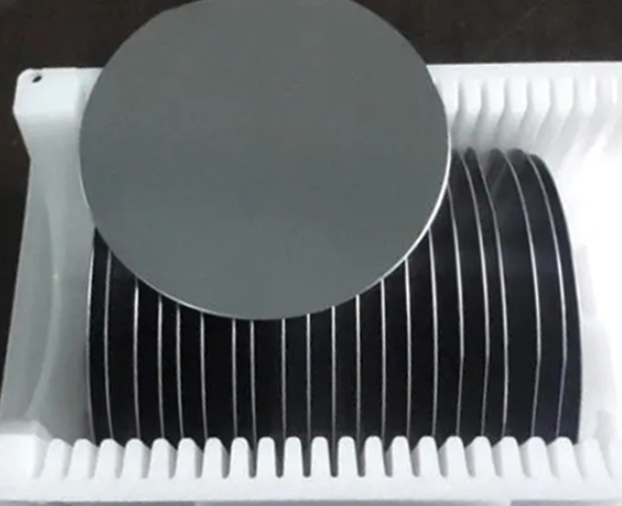
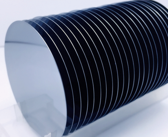
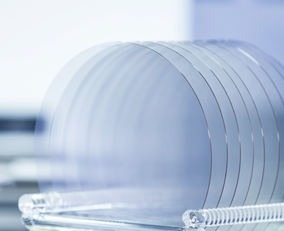
Chemical mechanical polishing (CMP) of semiconductor substrates is a key process in semiconductor manufacturing, mainly used to improve the flatness and smoothness of the substrate surface to meet the requirements of subsequent processes. The following is detailed information about CMP polishing of semiconductor substrates:
(1) Silicon materials
- Silicon is the most fundamental and widely used material in the semiconductor industry. The CMP process can effectively remove scratches, unevenness, and other defects on the surface of silicon wafers, improving surface flatness, which is crucial for subsequent chip manufacturing.
(2) Gallium arsenide and indium phosphide materials
- Gallium arsenide (GaAs) and indium phosphide (InP) are two important compound semiconductor materials widely used in high-frequency, high-speed electronic devices and optoelectronic devices.
(3) Silicon carbide materials
- Including wide bandgap semiconductor materials such as silicon carbide (SiC) and gallium nitride (GaN). These materials have wide applications in power electronics, microwave devices, etc., but their polishing processes are relatively complex and require specialized equipment and process parameters.
 Indium phosphide Indium phosphide |
 Gallium arsenide Gallium arsenide |
 Silicon wafer Silicon wafer |
 Silicon carbide Silicon carbide |
WanHua New Materials has the following polishing consumables in this field:


")
The CMP polishing technology of semiconductor substrates is an indispensable key process in semiconductor manufacturing, with applications covering various fields such as silicon materials, metal interconnect layers, dielectric layers, and special materials. With the continuous development of semiconductor technology, the CMP process will continue to evolve towards intelligence and efficiency to meet the demands for higher precision and more complex materials.
